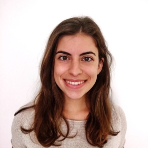
I am particularly interested in the synthesis and chemico-physical characterization of hybrid semiconductors for the study of carrier transport in perovskite semiconductors (PSC) by time-resolved spectroscopy with ultrashort visible and soft X-ray light. My fields of interest concern the integration of my knowledge in Physics and Nano Electronics for the conception of advanced materials with a condensed matter physics approach, and their characterization in the framework of time-resolved photoemission electron microscopy.
I graduated with a Master’s degree in Engineering physics at Politecnico di Milano. After my Bachelor’s Degree in Engineering Physics I decided to specialize my studies toward the fields of physics of matter and solid state physics. During that period, I got passionate in the study and characterization of magnetic, electrical and optoelectronic properties of low dimensional systems. After my first year of Master, I decided to start a Double Degree program in nano and opto-electronics in a Joint Master of École Polytechnique de Bruxelles (ULB) and the Faculty of Eng. Sciences(VUB). Thanks to this experience I adapted to a different methodology of studies and I got used to work and collaborate in team. I also had the opportunity to approach my fields of interest from another perspective, more oriented on the aspect of the final application of an optoelectronic device and on the fundamental aspects of material fabrication. I worked for one year in the section of Vacuum Surfaces and Coatings at CERN, this gave me the opportunity to experience a real research environment and to become familiar and independent with experimental instrumentation mostly for Ultra-High Vacuum (UHV). I learnt how to organize autonomously my work, within the framework of a project much more complex than those I faced during my academic career. The motivating and collaborative working environment allowed me to have useful and constructive discussions with physicists chemists and technicians of the team. I studied the outgassing of materials for applications under Ultra High Vacuum (UHV) and optimized their surface conductivity with metallic coatings deposited by magnetron sputtering in DC and HIPIMS configurations. This experience convinced me even more that research motivates me, when facing new challenges and failures. This doctoral program would allow me to put together what I learnt from my Masters in the fields of physics, optoelectronics and nanofabrication. I have now the opportunity to work in the framework of an European training network and specialize my knowledge in the field of ultrafast spectroscopy for the investigation of charge carrier dynamics.
EDUCATION
- Doctorate Studies in Physics 2020-2023; Istituto Italiano di Tecnologia (IIT), Milano, Italy and Dipartimento di Fisica, Politecnico di Milano, Milano, Italy
- MASTER’S DEGREE IN ENGINEERING PHYSICS – Nanophysics and nanotechnology. Politecnico di Milano, Milano, Italy
- MASTER’S DEGREE IN NANO, OPTO-ELECTRONICS. Joint Master of École Polytechnique de Bruxelles (ULB) and the Faculty of Eng. Sciences(VUB)
- BACHELOR IN ENGINEERING PHYSICS. Politecnico di Milano, Milano, Italy
PROJECTS AND RESEARCH EXPERIENCE
- Master Thesis October 2018-October 2019
TECHNICAL STUDENT AT CERN – Surface analysis and thin films for UHV group
Characterization of composite materials for UHV. Correlation of degassing properties in UHV through mass spectroscopy and microstructural and crystallographic characterization. Realization and characterization of metallic coatings deposited through magnetron sputtering in DC and HiPIMS configurations. Developement of models to simulate TDS desorption curves.
- GOLD NANOPARTICLES CHARACTERIZATION BY MEANS OF OPTICAL MICROSCOPY AND SURFACE PROBE MICROSCOPY TECHNIQUES Characterization of gold nanoparticles with AFM, SNOM and confocal microscopy
